Anna University
Engineering Physics 2
Unit 5
Modern Engineering Materials -SMA, Nanomaterials
Learning Objectives
On completion of this topic you will be able to understand:
1. Advantages of Shape memory Alloys
2. Disadvantages of Shape memory Alloys
3. Nanomaterials
4. Plasma arcing method to produce nanoparticles
Advantages and Disadvantages of Shape Memory Alloys
Some of the main advantages of shape memory alloys include:
• Bio-compatibility
• Diverse Fields of Application
• Good Mechanical Properties (strong, corrosion resistant)
There are still some difficulties with shape memory alloys that must be overcome before they can live up to their full potential. These alloys are still relatively expensive to manufacture and machine compared to other materials such as steel and aluminum. Most SMA's have poor fatigue properties; this means that while under the same loading conditions (i.e. twisting, bending, compressing) a steel component may survive for more than one hundred times more cycles than an SMA element.
Nanomaterials
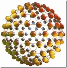
Nanomaterials are applications with morphological features smaller than a one tenth of a micrometre in at least one dimension. Materials referred to as "nanomaterials" generally fall into two categories: fullerenes, and inorganic nanoparticles.
The fullerenes are a class of allotropes of carbon which conceptually are graphene sheets rolled into tubes or spheres. These include the carbon nanotubes which are of interest both because of their mechanical strength and also because of their electrical properties.
Nanoparticles or nanocrystals made of metals, semiconductors, or oxides are of particular interest for their mechanical, electrical, magnetic, optical, chemical and other properties. Nanoparticles have been used as quantum dots and as chemical catalysts.
Production methods
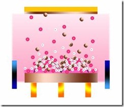
There are a number of methods of making CNTs and fullerenes. Fullerenes were first observed after vaporizing graphite with a short-pulse, high-power laser, however this was not a practical method for making large quantities. CNTs have probably been around for a lot longer than was first realized, and may have been made during various carbon combustion and vapor deposition processes, but electron microscopy at that time was not advanced enough to distinguish them from other types of tubes. The first method for producing CNTs and fullerenes in reasonable quantities – was by applying an electric current across two carbonaceous electrodes in an inert gas atmosphere. This method is called plasma arcing. It involves the evaporation of one electrode as cations followed by deposition at the other electrode. This plasma-based process is analogous to the more familiar electroplating process in a liquid medium. Fullerenes and CNTs are formed by plasma arcing of carbonaceous materials, particularly graphite. The fullerenes appear in the soot that is formed, while the CNTs are deposited on the opposing electrode.
Plasma Arc Method
The carbon arc discharge method, initially used for producing C60 fullerenes, is the most common and perhaps easiest way to produce CNTs, as it is rather simple. However, it is a technique that produces a complex mixture of components, and requires further purification - to separate the CNTs from the soot and the residual catalytic metals present in the crude product. This method creates CNTs through arc-vaporization of two carbon rods placed end to end, separated by approximately 1mm, in an enclosure that is usually filled with inert gas at low pressure. Recent investigations have shown that it is also possible to create CNTs with the arc method in liquid nitrogen. A direct current of 50 to 100 A, driven by a potential difference of approximately 20 V, creates a high temperature discharge between the two electrodes. The discharge vaporizes the surface of one of the carbon electrodes, and forms a small rod-shaped deposit on the other electrode. Producing CNTs in high yield depends on the uniformity of the plasma arc, and the temperature of the deposit forming on the carbon electrode.
Check your understanding
1. Crystal with size 109 is called nano material?
(a) Yes (b) No
Ans : No
2. The nano particles are free from crystal defects?
(a) Yes (b) No
Ans : Yes
Summary
1. SMAs are Bio-compatible, Diverse Fields of Application, Good Mechanical Properties (strong, corrosion resistant)
2. Nano materials are made of grains that are about 100nm (10-9) in diameter and contains less than thousands of atoms.
Suggested Reading
1. Palanisamy P.K, ‘Engineering Physics – II’ Scitech Publications (India) Pvt. LTd., Chennai – 17. (2009).
2. http://en.wikipedia.org/wiki/Nanomaterials


No comments:
Post a Comment